Trending
Opinion: How will Project 2025 impact game developers?
The Heritage Foundation's manifesto for the possible next administration could do great harm to many, including large portions of the game development community.
In the first of two articles to be reprinted from CMP sister publication Embedded Systems Design magazine, EIC Jim Turley offers an overview of the Cell processor, as used in Sony's upcoming PlayStation 3 console.
July 13, 2006

Author: by Jim Turley
Introduction
Remember your first time? Programming a processor, that is. It must have seemed both exciting and challenging.
You ain't seen nothing yet.
Even garden-variety microprocessors present plenty of challenges to an experienced programmer or development team. Now imagine programming nine different processors all at once, from a single source-code stream, and making them all cooperate. When it works, it works amazingly well. But making it work is the trick.
That's the task that IBM, Toshiba, and Sony took on several years ago in creating Cell, an amazing new multiprocessor microprocessor chip that will debut later this year in Sony's PlayStation 3 video game console, Toshiba's high-end televisions, and IBM's blade servers. Cell is the beginning of a new family tree for all three companies, and it promises to branch into consumer, computer, and embedded systems for many years to come. Let's take a look at what's inside the first Cell processor; for an insider's look at Cell's programming model, see Alex Chow's article [to appear on Gamasutra next week].
Insanely Complex, Insanely Cool
There aren't many businesses where manufacturing technology exceeds design technology. Throughout human history we've been able to dream up things we can't yet build, like spaceships, skyscrapers, jet packs, underwater breathing apparatus, or portable computers. But in the semiconductor business the situation is reversed: chip makers can build bigger and more complicated chips than they can design. Manufacturing prowess exceeds design capability. We can fabricate more transistors than we know what to do with.
Cell goes a long way toward ending that pattern. It's an insanely complex chip with about 250 million transistors (compared with 125 million for Pentium 4) that runs at more than 4GHz. With just the right conditions Cell can crank through 256 billion floating-point operations every second, according to IBM.
What's remarkable is that Cell wasn't developed for scientific applications, military computers, or code breaking. Instead, Cell is primarily intended for entertainment. It says a lot about embedded systems when three of the world's top multinational corporations devote millions of dollars in R&D and thousands of personnel into developing one of the world's most complex processors--for toys.
That's not to say that Cell can't also be used for more "serious" applications. As we'll see, Cell lends itself to parallel processing, which can be useful for scientific simulations and medical imaging. The fact that it also plays Gran Turismo is just a bonus.
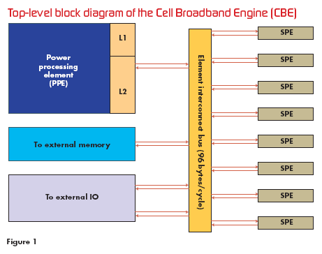
Figure 1 shows a top-level block diagram of the first processor in the Cell family, more formally known as the Cell Broadband Engine, or CBE. Cell is based around a single 64-bit PowerPC processor surrounded by eight identical coprocessors. The central PowerPC processor can execute two instructions at a time. That's nice, but not unusual. Intel, AMD, and others also produce dual-issue processors, even 64-bit dual-issue processors. So the heart of Cell is actually--dare we say it--fairly pedestrian.

Note that although the central processor is based on IBM's PowerPC architecture, it's a new design, not an existing PowerPC core. Cell's central processor is similar to the current PowerPC 970 chip, although it's not an exact match. The central processor includes the VMX (visual media extensions, similar to AltiVec) instruction-set extensions to the base PowerPC instruction set. The central processor has a pair of 32K first-level (L1) caches and a unified 512K second-level (L2) cache. This should keep the processor humming along at 4GHz.
Magic Eight Ball
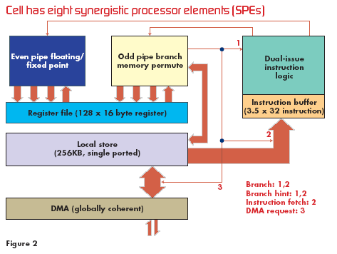
The real magic of cell lies with its eight "synergistic processor elements," or SPEs, shown in Figure 2. These are specially designed processors created from scratch by the IBM/Sony/Toshiba team just for Cell. They're not compatible with Power or PowerPC code in any way; they have their own distinct instruction set and internal architecture. For most code, and particularly for parallel vector operations, the SPEs do the heavy lifting. Each SPE is identical to its neighbors, and all share the same common bus with the central Power Processing Element (PPE in IBM-speak).
Like the central PowerPC processor, each SPE is a dual-issue machine but unlike the PPE the two execution pipelines are not symmetrical. In other words, each SPE can execute two instructions simultaneously but not two of the same instruction. The SPE's pipeline is "unbalanced," in that it can execute only arithmetic operations on one side (either fixed- or floating-point) and only logic, memory, or flow-control operations on the other side. That's not unusual; other superscalar processors have unbalanced pipelines, too. Most modern x86 chips, for example, have internal execution units dedicated to math, logic, or flow-control instructions and the hardware (or the compiler) determines how many of those can actually be used each cycle. It's the combination of these elements that determines the processor's ultimate performance and suitability to a task.

Each SPE is a 128-bit machine, with 128 registers that are each 128 bits wide. Its internal execution units are also 128 bits wide, which allows each SPE to handle either very large numbers or several small numbers at once. For example, each SPE can process two double-precision floats, four single-precision floats or long integers, eight 16-bit short integers, or 16 chars or other byte-sized quantities, all in a single cycle.
Although it stretches the definition considerably, each SPE has a RISC-like instruction set. They can load and store only quad-word (128-bit) quantities and all transactions must be on aligned addresses. If you want to load or store a byte or char, you've got to transfer the whole 16-byte quantity first and then mask off, merge, or extract the bits you want.
Each SPE actually has seven different execution units, although only two can be used at a time, as mentioned previously. Because one of the two execution pipelines is dedicated to arithmetic operations, an SPE can process fixed- or floating-point numbers nonstop while the other execution unit(s) in the other pipeline handle program flow. This reduces (but doesn't prevent) pipeline "bubbles" that get in the way of streaming data at top speed without interruption. Some DSP processors have similar internal architectures that separate program flow from data manipulation, and it works quite well most of the time. If the code tries to execute two arithmetic operations at once, the chip simply runs them in sequence instead of side-by-side. This isn't really a programming error but it does reduce the SPE's throughput considerably.
Internal Data Flow
Unlike the PPE, the SPEs do not have caches. Instead, they each get a 256K "local store" that only they can see. All code and data for the SPE must be stored within this 256K local area. In fact, the SPEs cannot "see" the rest of the chip's address space at all. They can't access each others' local stores nor can they access the PPE's caches or other on-chip or off-chip resources. In effect, each SPE is blind and limited to just its own little corner of the Cell world.
Why the crippled address map? Each SPE is limited to just a single memory bank with deterministic access characteristics in order to guarantee its performance. Off-chip (or even on-chip) memory accesses take time--sometimes an unpredictable amount of time, and that goes against the SPE's purpose. They're designed to be ultra-fast and ultra-reliable units for processing streaming media, often in real-time situations where the data can't be retransmitted. By limiting their options and purpose, Cell's designers gave the SPEs deterministic performance.
This is where the DMA controllers come in. Each SPE has its own 128-bit wide DMA controller (64 bits in, 64 bits out) between it and Cell's local bus. The PPE and all eight SPEs share the same bus, called the Element Interconnect Bus (EIB). Through this bus each DMA controller fetches the instructions and data that its attached SPE will need. The DMA controller also pushes results out onto the shared bus, where it can be exported off-chip, sent to on-chip peripherals, or cached by the PPE.
The central processor's L1 and L2 caches snoop the EIB, so the caches are always fully coherent. The SPEs do not snoop the bus; in fact, they don't monitor bus traffic at all. That means that the central PowerPC processor is aware of what data the SPEs may transfer but the SPEs are totally unaware of any traffic amongst their neighbors. Again, this keeps the SPEs relatively simple and limits interruptions or unwanted effects on their behavior. If the SPEs need to be made aware of external data changes, their respective DMA controllers will have to fetch it. And that, presumably, would be under the control of the central PPE.
Super Cell
Mere mortals can program the Cell processor but it's a unique experience. A handful of embedded systems developers already have experience programming multiprocessor systems; some have even coded multicore processors. But Cell promises to up the game. Each of the chip's nine individual processor elements is itself a dual-issue machine with complex pipeline interlocks, cache-coherence issues, and synchronization problems. Keeping all eight SPEs fed at once promises to be a real chore. Yet the results are bound to be spectacular. If your application can benefit from sustained high-speed floating-point operations and can be parallelized across two or more SPEs you should be in for a real treat. That is, once you get the code running.
IBM is working on an "Octopiler" that compiles C code and balances it across Cell's eight SPEs. Tools like that, and like the ones described in our companion article on page 18, are absolutely necessary if Cell is to be a success. To take another example from the video game industry, Sega's Saturn console was a failure largely because its four-processor architecture (three SuperH chips and a 68000) was too difficult to program. Developers working under tight deadlines simply ignored much of the system's power because they couldn't harness it effectively. Cell brings that problem in spades. It's an impressive achievement in computer architecture and semiconductor manufacturing. Products based on Cell promise to be equally impressive. But bringing Cell to life will require real software alchemy.
Jim Turley is editor in chief of Embedded Systems Design magazine. You can reach him at [email protected].
Read more about:
FeaturesYou May Also Like